Introduction
In the process of qualification, debugging and testing of complex systems a source of random data is often needed while access to authentic data stream is difficult or impossible. Usually, such signals are generated and analysed using bulky and expensive equipment. Compact and low-cost on-chip equivalent would be advantageous. Such solution is an on-chip PRBS generator and checker, producing test signals mimicking genuine data streams. Data signals are random by nature, while PRBS signals are ruled by mathematical formulas. For instance, PRBS-7 runs according to X=(X+6)^(X+7) formula and PRBS-31 according to X=(X+28)^(X+31) formula. Signals generated this way poses properties that make them useful for some applications. Since there is a firm relation between bits in the PRBS signal, this kind of bit stream can “reference itself” rather than use some original reference signal to which the verified/tested signal must be synchronized and compared. Such synchronization must be bit-to-bit and therefore is complicated. In order to identify an error (an altered bit in the sequence) it’s enough to just check if all the bits in tested PRBS signal are following the mathematical rule. Another useful property of PRBS is that it has finite length, after 2^N-1 symbols PRBS of Nth order will repeat itself. Another property is that within the full 2^N-1 bit length PRBS-N will have all possible combination of “1s” and “0s” within N-bit patterns and will not have more then N bits of consecutive “0s” or more then N-1 bits of consecutive “1s” which corresponds to many communication standards restricting length of Consecutive Identical Digits (CID) in telecommunication channels. All the properties of PRBS make these signals useful as deterministic signals for telecommunication system testing and other applications. A simple example of a PRBS generator circuit is shown in FIG.1.

FIG. 1: Basic PRBS generator circuit
Telecommunication applications
One important figure of merit in a telecommunication system is Bit Error Rate or BER, which counts number of errors (altered bits) per certain number of transmitted bits. Knowing BER helps to understand whether a telecommunication channel has too much attenuation, noise or crosstalk resulting in transmitted signal distortion and errors. Also, whether the telecommunication system (such as SerDes or CDR) has the capability to restore received signal, so that use of error correction algorithms is efficient or resending packages is minimized. PRBS is a very good fit for testing telecommunication systems measuring BER. Below are a few examples of PRBS generator and error counter can be used in such systems.
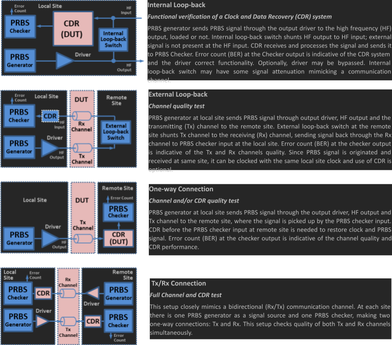
FIG. 2: Examples of telecommunication applications of PRBS generator/checker
Memory testing application
While standalone memory ICs can be tested using specialized memory testing equipment, testing of embedded memory arrays may be difficult, especially when variety of memory types are placed on same chip. In ASICs using memory arrays (such as on-chip DRAM, SRAM and other types of embedded storage) Built-in Self Test (BIST) is often implemented. Such BIST may use PRBS generator and checker as source of random pattern data as well as error locator. In memory arrays signal latency is well controlled and so is PRBS generator/checker which essentially is a synchronous pipeline. Controlled latency helps to maintain accurate bit count in a bit stream and to establish exact correspondence between bit in the stream and exact location in the memory where the bit was stored and potentially distorted/altered. FIG.3 below shows an example of PRBS generator/checker used in embedded memory testing. PRBS generates a stream of bits at high frequency which is parallelized by S2P and sent to a storage array at low frequency. Once the array is filled, the PRBS switches to checker mode and data is read back from the array, serialized by P2S and run through the checker. Checker registers distorted bits and by knowing exact signal latencies in the data path identifies faulty memory locations that must be replaced engaging redundancy mechanisms. This process may be repeated several times with the bit stream shifted to ensure that all cells in the storage receive a variety of bit combinations and this can be done easily since all necessary testing gear is on-chip and no expensive external equipment or elaborate interface circuitry is required. As an optional configuration, when memory volume is larger then full PRBS sequence of 2^N-1 bits, same PRBS core may be used as generator and checker cycling the bit flow, making process continuous and reducing test time. This scheme requires circuitry to maintain strict order of bits for the PRBS unit to work correctly.
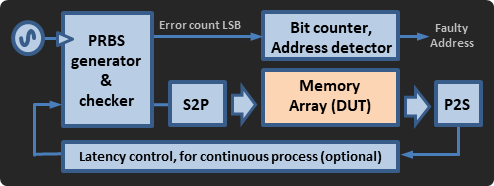
FIG. 3: PRBS generator/checker in embedded memory testing system
CDR pre-locking application
Locking time of a CDR may be long and can start only after received signal had been restored to good quality which also could take considerable time. If there are interruptions in the received signal, the CDR locking process has to be repeated. To shorten the locking process, an at-speed pseudo-random signal can be used to pre-lock CDR and make it ready to switch to the restored signal of the same frequency once the CDR is in lock. A simpler PRBS generator as shown in FIG,1 could suffice.
If a more complex fast PRBS unit is already present in the system, it can also be used for this purpose. A block diagram of PRBS for CDR pre-lock is shown in FIG. 4. While data path (including CTLE, DFE and PGA) restores received signal, the process of CDR pre-locking is also going on. The 2 processes running simultaneously help to shorten startup and power up of the CDR. With minor modifications this circuit can also keep CDR in lock while received signal is interrupted or not available.
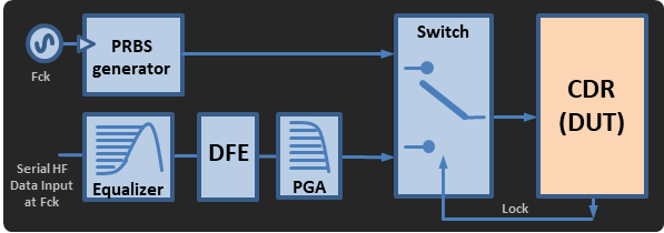
FIG. 4: PRBS generator used for CDR pre-lock
PRBS Generator and Checker by Kamaten
Kamaten Technology offers PRBS generator/checker – multifunctional IP cores capable of all PRBS functions described above: generating PRBS signal, checking it for errors, accurately counting and correcting the errors, producing error free PRBS signal, while checking and correcting and switching to power down mode when not used. Our PRBS cores are compact and efficient with simple low frequency asynchronous control interfaces making them easy to use. The units can produce PRBS streams of 7, 15 and 31 order at 32Gsps data/symbol rate and higher. Error count by Kamaten PRBS units is accurate: no error will escape count or counted more then once, regardless of how frequently and in what order errors occur in the input PRBS signal. All high frequency input and output signals as well as all low frequency control signals are CMOS. FIG. 5 shows main signals of the units: first from the top is reset, next below is output enable. Third is PRBS signal that appears at differential data output (only one polarity shown). Just below the output signal is error injection mask – high level injects an error into PRBS signal at the unit input (not shown). Errors in this example occur very frequently, total count of the injected errors is 50. The next 4 waveforms below are control signals applied in a simple sequence to enable signal generation, error count and correction. At the bottom of the diagram is an analog representation of the 10-bit ripple error counter output code which may be read reliably after all ripples settle. About 6-7ns after last injected error the waveform settles at 50mV value with digital-to-analog conversion 1 error = 1mV meaning that exactly 50 errors were counted, exactly matching the 50 injected errors. More information can be found in the Application Notes.
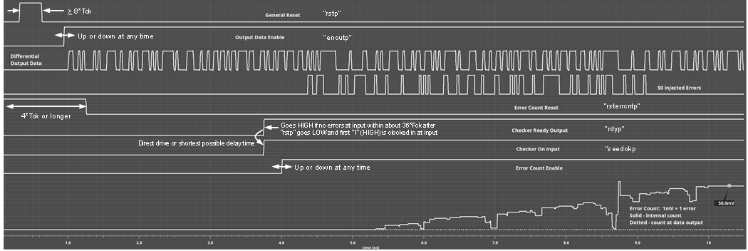
FIG. 5: Kamaten PRBS unit main signals
FIG. 6: Kamaten PRBS output data eye
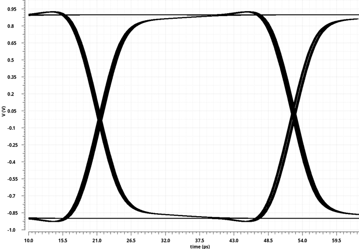
FIG.6 shows a differential eye diagram at the PRBS generator data output, simulated at temperature +40C, power supply voltage 0.9V, all typical process parameters and with 16GHz input differential clock. In error checking mode the clock captures PRBS signal at the input using DDR signalling order. To facilitate the use of the output signal PRBS unit generates 32GHz differential CMOS output clock aligned with the output data. Higher then 32Gbps data rates may be achieved with processes more advanced than 28nm.
At this time Kamaten offers PRBS generator/checker implemented in TSMC 28nm HPC/HPC+ process. Design in 16nm is being developed and will be migrated to more advanced process nodes.
More detailed information about Kamaten’s family of PRBS generator/checker IP cores may be obtained by contacting info@kamaten.com or visiting www.kamaten.com .